Digital Electronics
ACSL digital electronics problems give you a circuit diagram made of logic gates and ask you to find the output, simplify the circuit, or determine which inputs produce a given output. This is Boolean algebra made physical - the same rules apply, but now you’re reading a diagram instead of an equation.
The gates
Every gate takes one or more binary inputs (0 or 1) and produces one binary output.
BUFFER gate
One input, one output. Output equals the input with no change. Rarely appears alone in problems, but is part of the official gate set.

| In | Out |
|---|---|
NOT gate (inverter)
One input, one output. Flips the bit.

| In | Out |
|---|---|
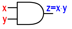
AND gate
Output is 1 only when all inputs are 1.
| A | B | Out |
|---|---|---|
OR gate
Output is 1 when any input is 1.

| A | B | Out |
|---|---|---|
NAND gate (NOT AND)
The opposite of AND. Output is 0 only when all inputs are 1. The small circle on the output means “invert.”

| A | B | Out |
|---|---|---|
NOR gate (NOT OR)
The opposite of OR. Output is 1 only when all inputs are 0.

| A | B | Out |
|---|---|---|
XOR gate
Output is 1 when inputs differ.

| A | B | Out |
|---|---|---|
XNOR gate (NOT XOR)
Output is 1 when inputs are the same.

| A | B | Out |
|---|---|---|
Note: there is some ambiguity when converting a diagram to a Boolean expression. For example, could be an OR gate followed by a NOT gate, or simply a NOR gate. ACSL problems will make the intended circuit clear from the diagram.
Reading a circuit diagram
Work left to right (inputs to output), evaluating one gate at a time.
Example:
A ──┐
    AND──┐
B ──┘    OR── Output
C ───────┘
Step 1: AND gate takes A and B. Output . Step 2: OR gate takes and C. Output .
If , , :
- AND:
- OR:
Output = 1
Multi-layer circuits
For deeper circuits with several layers of gates, label intermediate wires.
Example:
A ──┐
    AND── W1 ──┐
B ──┘          OR── W3 ──▷○── Output
C ──┐          │
    OR── W2 ───┘
D ──┘
W1 = A AND B = W2 = C OR D = W3 = W1 OR W2 = Output = NOT W3 =
Speed tip: Label each gate’s output as you go. Don’t try to hold everything in your head.
From circuit to Boolean expression
Trace from inputs to output, writing the expression for each gate:
- Start at the final output gate
- Write what that gate does to its inputs
- Replace each input with its sub-expression
- Simplify using Boolean algebra laws
Example:
A ─▷○── NOT_A ──┐
                 AND── Output
B ───────────────┘
Output
From Boolean expression to circuit
Go the other direction - break the expression into gates:
For :
- OR gate: inputs A and B, output
- NOT gate: input C, output
- AND gate: inputs and , output
Truth table from circuit
For problems asking “find all inputs that produce output 1,” build a truth table.
Example: Circuit implements
| A | B | C | |||
|---|---|---|---|---|---|
Output is 1 for inputs: (0,0,1), (0,1,1), (1,1,0), (1,1,1).
Reasoning backward (faster method)
For circuits with many inputs, truth tables get large (4 inputs = 16 rows). Instead, reason backward from the output gate.
Example: Find all inputs that make this circuit FALSE:
A ──┐
    NAND──┐
B ──┘      OR── Output
C ─────────┘
The circuit is . For this to be FALSE, the OR gate must output 0, which means both its inputs must be 0:
- (one input to OR must be 0)
- , which means , so and
Only one answer: (1, 1, 0)
This took 3 lines of reasoning instead of an 8-row truth table.
Circuit simplification
If a circuit is complex, write the Boolean expression, simplify using Boolean algebra (see the Boolean Algebra lesson), then redraw.
Example: A circuit implements .
Simplify:
The simplified circuit is just an OR gate with inputs A and B.
Common mistakes
- Forgetting the inversion bubble. The small circle on NAND/NOR/NOT gates flips the output. Missing it changes everything.
- Wrong gate read. AND vs OR confusion under time pressure. Double-check each gate symbol.
- Evaluating gates in wrong order. Always work from inputs toward output, layer by layer.
- DeMorgan’s in circuits. A NAND gate is , not .
- Assuming left-to-right is top-to-bottom. Read the actual wire connections, not the visual position.
Contest strategy
- Label every intermediate wire with its value (when evaluating) or expression (when deriving)
- For “find the output” problems: plug in values left to right, gate by gate (~30 seconds)
- For “write the expression” problems: trace from output back to inputs (~45 seconds)
- For “simplify” problems: get the expression first, then use Boolean algebra laws (~60-90 seconds)
- For truth table problems with 2 variables, just enumerate all 4 cases. With 3 variables, all 8 cases.
- Typical time: 45-90 seconds depending on problem type